SEM EDX / EDS Analysis or Scanning Electron Microscopy & Energy Dispersive X-Ray Spectroscopy Analysis.
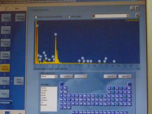
Scanning Electron Microscopy (SEM) has the advantage over optical microscopy of working at greater resolutions and magnifications. The SEM at ITA Labs is fitted with an Energy Dispersive X-Ray (EDX) detector for the elemental compositional information during inspection of a sample.
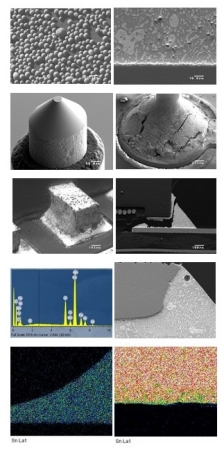 As a surface sensitive technique, the electron microscopy can be used in applications where topographic information is important, such as for coating textures or for powder characterisation, where the imaging capability provides information on uniformity, size and shape.
For examination in cross-section, SEM is integral for solder joint evaluations, where the inter-facial bond between the solder and PCB is particularly important.
EDX / EDS allows quick, semi-quantitative sample characterisation and can be used to identify surface contamination and impurities located by the SEM examination. EDX / EDS is also required to ascertain if the correct material has been used in the manufacture of a product, e.g. grade of alloy.
This form of fractography is frequently used to establish the cause of product failures and in the practice of forensic engineering, or failure analysis.
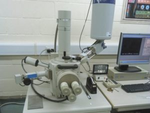
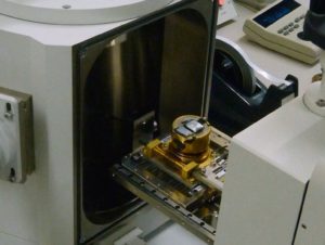
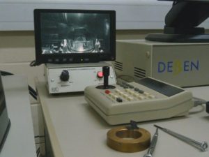
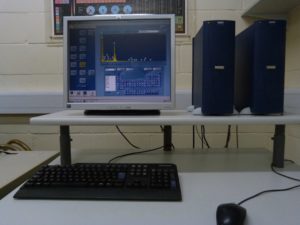
The electron optics suite at ITA Labs is a Topcon SM300 SEM, equipped with an Oxford Instruments x-act detector and Aztec EDX software system. This has recently been updated with a motorized stage which improves our capabilities.
 |
 |
 |
|
 |
 |
ITA Labs’ UK laboratory SEM-EDX analysis service is extremely experienced at providing SEM / EDX test results, with a fast turnaround, at very competitive rates using a Topcon SM300 scanning electron microscope.
To discuss your potential requirements, contact Tony at tony.wallace@internationaltin.org

+44 (0)1727 871326